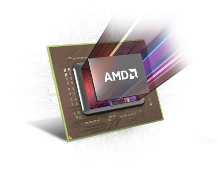
AMD Discloses Architecture Details of High-Performance, Energy-Efficient “Carrizo” System-on-Chip
SYDNEY, Australia. — February 25, 2015 — AMD (NASDAQ:AMD) revealed at the prestigious International Solid State Circuits Conference (ISSCC) that the upcoming A-Series Accelerated Processing Unit (APU), codenamed “Carrizo”, for notebooks and low-power desktops will deliver a wealth of new, advanced power management technologies while achieving substantial performance through new “Excavator” x86 CPU cores and a new generation of AMD Radeon™ GPU cores. Using a true System-on-Chip (SoC) design, AMD expects Carrizo to reduce the power consumed by the x86 cores alone by 40 percent, while also providing substantial gains in CPU, graphics, and multimedia performance over the prior generation APU.
“As a part of our continued focus on building great products, the advanced power and performance optimisations we have designed into our upcoming ‘Carrizo’ APU will deliver the largest generational performance-per-watt gain ever for a mainstream AMD APU,” said Sam Naffziger, AMD Corporate Fellow and co-author of the AMD presentation at ISSCC. “There have been remarkable advances in performance and energy efficiency in computing since the birth of the modern microprocessor. However, the energy-related benefits that flow from new manufacturing processes have slowed, ushering in an era when alternative ways to improve processor performance and efficiency are needed. AMD has been pursuing Heterogeneous System Architecture (HSA) and proprietary power management technologies to make continued gains. The upcoming ’Carrizo’ APU takes a big step toward the AMD 25×20 energy efficiency goal and incorporates a wealth of new features that will be adopted across our full product line going forward.”
New Carrizo Disclosures at ISSCC:
• 29% more transistors in nearly the same die size as its predecessor, “Kaveri”;
• New “Excavator” x86 cores provide an uplift in instructions-per-clock at 40% less power;
• New Radeon GPU cores with dedicated power supply;
• Dedicated, on-chip H.265 video decode;
• Double digit percentage increases in both performance and battery life;
• Integrated Southbridge for the first time on an AMD high-performance APU.
Details will be presented today at the AMD ISSCC session, “A 28nm x86 APU Optimised for Power and Area Efficiency,” by AMD Fellow and Design Engineer Kathy Wilcox. The presentation covers the technology, implementation, and power management features of the Carrizo APU.
Architectural Advances
New high density design libraries allowed AMD to fit 29 percent more transistors on Carrizo – 3.1 billion – in nearly the same chip size as the previous generation, Kaveri APU. This density increase has allowed a larger area for graphics, multimedia offload, and integration of the “Southbridge” system controller on a single-chip. The increased support for multimedia includes the new, high-performance H.265 video standard and double the video compression engines of its predecessor. The inclusion of H.265 in hardware will support true 4K resolutions, help extend battery life, and reduce bandwidth requirements when viewing compatible video streams.
The additional transistor budget also allows Carrizo to become the first processor in the industry designed to be compliant with the HSA 1.0 specification developed by the HSA Foundation. HSA makes programming accelerators such as the GPU far simpler, ideally leading to greater application performance at low power consumption.
Chief among the design advantages for HSA is the heterogeneous Unified Memory Access (hUMA) within Carrizo. With hUMA, the CPU and GPU share the same memory address space. Both can access all the platform’s memory and allocate data to any location in the system’s memory space. This coherent-memory architecture greatly reduces the number of instructions required to complete many tasks, thus helping improve both performance and energy efficiency.
New Energy Efficient Features
Several new power efficient technologies make their debut on the Carrizo APU. To deal with transient drops in voltage, which is known as droop, traditional microprocessor designs supply excess voltage on the order of ten to fifteen percent to ensure the processor always has appropriate voltage. But over-voltage is costly in terms of energy because it wastes power at a rate that is proportional to the square of the voltage increase. 1(i.e. 10% over-voltage means about 20% wasted power).
AMD has developed a number of technologies to optimise voltage. Its latest processors compare the average voltage to droops on the order of nanoseconds, or billionths of a second. Starting with the Carrizo APU, this voltage adaptive operation functions in both the CPU and the GPU. Since the frequency adjustments are done at the nanosecond level, there’s almost no compromise in computing performance, while power is cut by up to 10 percent on the GPU and up to 19% on the CPU.
Another power technology that debuts in Carrizo is called adaptive voltage and frequency scaling (AVFS). This technology involves the implementation of unique, patented silicon speed capability sensors, and voltage sensors in addition to traditional temperature and power sensors. The speed and voltage sensors enable each individual APU to adapt to its particular silicon characteristics, platform behaviour, and operating environment. By adapting in real time to these parameters, AVFS can lead to up to 30 percent power savings.
In addition to helping reduce power use on the CPU by shrinking the core area, AMD worked to optimise the 28nm technology for power efficiency, and tuned the GPU implementation for optimal operation in power limited scenarios. This enables up to a 20% power reduction over the Kaveri graphics at the same frequency. Combined, AMD’s energy efficiency innovations aim to deliver power savings on the order of a manufacturing technology shrink while staying in a well-characterised, cost-optimised 28nm process.


